Sunday, August 15, 2010

A chlorine molecule forms a covalent bond


Modern electronics can trace its roots to the first electronic devices called vacuum tubes. Although, today, solid state devices have totally replaced the vacuum tube, the fundamental principle as to its usage remains relatively unchanged. For more than 40 years, until the late 1960s, the most important part in a consumer electronics product was the vacuum tube. It is with this historical perspective in mind that this section is presented so that readers will not lose sight of where it all started.


The vacuum tube got its start in 1883, when Edison was developing the incandescent lamp. To correct the premature burnout of the red-hot filament in light bulbs, Edison tried a number of experiments, one of which was to place a metal plate sealed inside a bulb and connect it to a battery and ammeter, as shown in Fig. 1.4. Edison observed that, when the filament was hot and the plate was positively (+) charged by the battery, the ammeter indicated a current flow through the vacuum, across the gap between the filament and the plate. When the charge on the plate was reversed to negative (–), the current flow stopped. As interesting as this phenomena was, it did not improve the life of Edison’s lamps and, as a result, he lost interest in this experiment and went on to other bulb modifications that proved more successful. For about 20 years, Edison’s vacuum tube experiment remained a scientific curiosity. In 1903, as radios were coming into use, J. A. Fleming, in England, found just.

Bohr model of silicon atom


Electrons are being forced into the next higher shell. An atom is chemically stable if its outer shell is either completely filled with electrons, based on the 2n2 rule, or has eight electrons in it. The electrons in the outer shell are called valence electrons and, if their number is less than eight, the atom will have a tendency to interact with other atoms either by losing, acquiring, or merging its electrons with other atoms. In the periodic table (Fig. 1.1), elements with the same number of valence electrons have similar properties and are placed in the same group. For example, elements in Group I have atoms with one electron in their outer shell. Group II shows elements that have atoms with two electrons in their outer shell, and so on. Elements on the left side of the periodic table have a tendency to lose their valence electrons to other atoms, thus becoming electropositive. The elements on the right side of the periodic table show a tendency to acquire electrons from other atoms and become electronegative.
The type of interaction occurring between atoms, as they are brought together, depends largely on the properties of the atoms themselves. The interaction may form bonds that can be classified as ionic, covalent, molecular, hydrogen bonded, or metallic. Since this chapter is concerned with semiconductors, which tend to form covalent bonds with other elements and with themselves, the emphasis will be on covalent bonding. Covalent bonds occur when two or more atoms jointly share each other’s valence electrons. If the outer shell is partially filled with electrons, the atom will be attracted to other atoms also having a deficiency of electrons, so sharing each other’s valence electrons will result in a more stable condition. As an example, two chlorine atoms will attract and share each other’s single electron to orm a stable covalent bond with eight electrons in each shell (Fig. 1.3).

Friday, July 23, 2010

IDEAL DIODE

The first electronic device to be introduced is called the diode. It is the simplest of semiconductor devices but plays a very vital role in electronic systems, having characteristics that closely match those of a simple switch. It will appear in a range of applications, extending from the simple to the very complex. In addition to the details of its construction and characteristics, the very important data and graphs to be found on specification sheets will also be covered to ensure an understanding of the terminologyemployed and to demonstrate the wealth of information typically available from manufacturers.
The term ideal will be used frequently in this text as new devices are introduced. It refers to any device or system that has ideal characteristics—perfect in every way. It provides a basis for comparison, and it reveals where improvements can still be made. The ideal diode is a two-terminal device having the symbol and characteristics shown in Figs. 1.1a and b, respectively. Ideally, a diode will conduct current in the direction defined by the arrow in the symbol and act like an open circuit to any attempt to establish current in the opposite direction. In essence:

The characteristics of an ideal diode are those of a switch that can conduct current in only one direction.


In the description of the elements to follow, it is critical that the various letter symbols, voltage polarities, and current directions be defined. If the polarity of the applied voltage is consistent with that shown in Fig. 1.1a, the portion of the characteristics to be considered in Fig. 1.1b is to the right of the vertical axis. If a reverse voltage is applied, the characteristics to the left are pertinent. If the current throughthe diode has the direction indicated in Fig. 1.1a, the portion of the characteristics to be considered is above the horizontal axis, while a reversal in direction would require the use of the characteristics below the axis. For the majority of the device characteristics hat appear in this book, the ordinate (or “y” axis) will be the current axis, while the abscissa (or “x” axis) will be the voltage axis.
One of the important parameters for the diode is the resistance at the point or region of operation. If we consider the conduction region defined by the direction of ID and polar  of VD in Fig. 1.1a (upper-right quadrant of Fig. 1.1b), we will find that the value of the forward resistance, RF, as defined by Ohm’s law is


where VF is the forward voltage across the diode and IF is the forward current through The ideal diode, The ideal diode, therefore, is a short circuit for the region of conduction. Consider the region of negatively applied potential (third quadrant) of Fig. 1.1b,


where VR is reverse voltage across the diode and IR is reverse current in the diode.The ideal diode, therefore, is an open circuit in the region of nonconduction. In review, the conditions depicted in Fig. 1.2 are applicable.

In general, it is relatively simple to determine whether a diode is in the region of conduction or nonconduction simply by noting the direction of the current ID established by an applied voltage. For conventional flow (opposite to that of electron flow), if the resultant diode current has the same direction as the arrowhead of the diode symbol, the diode is operating in the conducting region as depicted in Fig. 1.3a. If  the resulting current has the opposite direction, as shown in Fig. 1.3b, the opencircuit equivalent is appropriate.


As indicated earlier, the primary purpose of this section is to introduce the characteristics of an ideal device for comparison with the characteristics of the commercial variety. As we progress through the next few sections, keep the following questions in mind:

How close will the forward or “on” resistance of a practical diode compare with the desired 0- level? Is the reverse-bias resistance sufficiently large to permit an open-circuit approximation?

Semiconductor Diodes INTRODUCTION

It is now some 50 years since the first transistor was introduced on December 23, 1947. For those of us who experienced the change from glass envelope tubes to the solid-state era, it still seems like a few short years ago. The first edition of this text contained heavy coverage of tubes, with succeeding editions involving the important decision of how much coverage should be dedicated to tubes and how much to semiconductor devices. It no longer seems valid to mention tubes at all or to compare the advantages of one over the other—we are firmly in the solid-state era. The miniaturization that has resulted leaves us to wonder about its limits. Complete systems now appear on wafers thousands of times smaller than the single element of earlier networks. New designs and systems surface weekly. The engineer becomes more and more limited in his or her knowledge of the broad range of advances— it is difficult enough simply to stay abreast of the changes in one area of research or development. We have also reached a point at which the primary purpose of the container is simply to provide some means of handling the device or system and to provide a mechanism for attachment to the remainder of the network. Miniaturization appears to be limited by three factors (each of which will be addressed in this text): the quality of the semiconductor material itself, the network design technique, and the limits of the manufacturing and processing equipment.

Tuesday, July 20, 2010

Sharp to join e-reader business war

A man looks at e-book products on display at a booth of Taiwan's Green Book Inc, during the five-day Computex Taipei in June. Sharp said it would launch an e-reader this year able to handle text as well as video and audio content, in a bid to challenge Apple and other rivals in the lucrative market.

Sharp said Tuesday it would launch an e-reader this year able to handle text as well as video and audio content, in a bid to challenge Apple and other rivals in the lucrative market.


The Japanese electronics giant said it had updated its e-book format with the "next-generation XMDF" platform, an advanced multimedia version of the XMDF format for text and still images that it launched in 2001.
"The next-generation XMDF enables easy viewing of digital content including video and audio and allows automatic adjustment of the layout to match and meet publishers' needs," Sharp said in a statement.
Sharp plans to begin the service and sell two types of e-readers, which resemble Apple's and , by the end of the year in Japan and will then also export the gadgets.
"Now there is a lot of attention on the e-publishing business," Masami Obatake, a senior Sharp official, told a news conference. "Launching it by the end of this year will be good timing."
Asked if Sharp can cope with the competition, Obatake said: "Since we have a new system, I think we will be able to compete sufficiently."
Sharp said it had already reached basic accords with major Japanese publishers and newspaper companies on content, adding it would be open to further collaboration to establish an e-book market.
In late May, Sony announced a similar plan jointly with telecoms operator KDDI, the Asahi Shimbun newspaper company and the Toppan printing company, with each company taking a 25 percent stake.
That came just a day before the launch of the iPad in Japan and other countries outside the United States, where print media face a steady decline in advertising and have turned to e-readers as a way to win new revenue.
The Japanese market is now estimated to be worth 46 billion yen (about 500 million dollars), with most titles distributed via and conventional computers.
Japanese news media had until this year taken a wait-and-see approach to the devices, contrary to US peers.
Newspaper circulation has held up better than in the United States, having fallen only six percent between 1999 and 2009 to 50.3 million sales daily, the Japan Newspaper Publishers & Editors Association said. However, magazine circulation in Japan has slumped by a third over the decade.

Sourch

12-Bit or line or Way input-output system for Robotic

This is a circuit which works 12-Bit or line or Way input-output system for Robotic. You can use this in your Robotic porjects.


2 x 4081 AND gate
2 x 4030 NOR gate
2 x ULN2803 Driver
1 x 74LS244 buffer
12 x 560 ohm resistor
12 x 100Kohm resistor
1 x 10Kohm resistor
1 x 47 uF electrolytic capacitor
1 x 2.1mm power socket
1 x DB25 PCB mount, right angle socket
1 x serial cable (male to male)
1 x 1 amp bridge rectifier
1 x 7805 voltage regulator
1 x 7812 voltage regulator
12 x 3mm red LEDs
2 x 0.01 uF greencap capacitors
1 x PCB

Sourch

Robotic Pictures

CDbot Robot:


Surveyor Stereo Vision System:


Self Balancing Segway  Robot


Mini Segway Using Arduino:


RF Modem Robotics Project:


Sourch

Low Cost Switcher Converts 5 to 24V

This is a simple circuit. which is Low cost switcher converter 5v to 24v by using OPamp.

Sourch

A very simple Inverter circuit - 12 volt DC to 120 volt AC

This is a very simple inverter circuit. This Inverter takes 12 volt d.c and steps it up to 120 volt a.c. The wattage depends on which transistors you use for Q1 and Q2, as well as the "Amp Rating" of the transformer you use for T1. This inverter can be constructed to supply anywhere from 1 to 1000 (1 KW) watts. If Q1, Q2 are 2N3055 NPN Transistors and T1 is a 15 A transformer, then the inverter will supply about 300 watts. Larger transformers and more powerful transistors can be substituted for T1, Q1 and Q2 for more power.


Parts List:

C1, C2 --------------------- 68 uf, 25 V Tantalum Capacitor

R1, R2 --------------------- 10 Ohm, 5 Watt Resistor

R3, R4 --------------------- 180 Ohm, 1 Watt Resistor

D1, D2 --------------------- HEP 154 Silicon Diode

Q1, Q2 --------------------- 2N3055 NPN Transistor (see "Notes")

T1 ---------------------------- 24V, Center Tapped Transformer

Others:

Wire, Case, Receptacle (for output)

Fuses, Heatsinks, etc.


Note: Don't try to connect this inverter with loads motors .

Sourch

Mains Switch Manager


Introduction:

Very often we forget to switch of the peripherals like monitor, scan ner, and printer while switching of our PC. The problem is that there are separate power switches to turn the peripherals off. Normally, the peripherals are connected to a single of those four-way trai ing sockets that are plugged into a singl wall socket. If that socket is accessible, a the devices could be switched off from there and none of the equipment used wi require any modification.


Description:

Here is a mains manager circuit that allows you to turn all the equipment on or off by just operating the switch on any one of the devices; for example, when you switch off your PC, the monitor as well as other equipment will get powered down automatically. You may choose the main equipment to control other gadgets. The main equipment is to be directly plugged into the master socket, while all other equipment are to be connected via the slave socket. The mains supply from the wall socket is to be connected to the input of the mains manager circuit.

Operation:

The unit operates by sensing the current drawn by the control equipment/load from the master socket. On sensing that the control equipment is on, it powers up the other (slave) sockets. The load on the master socket can be anywhere between 20 VA and 500 VA, while the load on the slave sockets can be 60 VA to 1200 VA.

During the positive half cycle of the mains AC supply, diodes D4, D5, and D6 have a voltage drop of about 1.8 volts when current is drawn from the master socket. Diode D7 carries the current during negative half cycles. Capacitor C3, in series with diode D3, is connected across the diode combination of D4 through D6, in addition to diode D7 as well as resistor R10. Thus current pulses during positive half-cycles, charge up the capacitor to 1.8 volts via diode D3. This voltage is sufficient to hold transistor T2 in forward biased condition for about 200 ms even after the controlling load on the master socket is switched off.

When transistor T2 is ‘on’, transistor T1 gets forward biased and is switched on. This, in  turn, triggers Triac 1, which then powers the slave loads. Capacitor C4 and resistor R9 form a snubber network to ensure that the triac turns off cleanly with an inductive load.

LED1 indicates that the unit is operating. Capacitor C1 and zener ZD1 are effectively in series across the mains. The resulting 15V pulses across ZD1 are rectified by diode D2 and smoothened by capacitor C2 to provide the necessary DC supply for the circuit around transistors T1 and T2. Resistor R3 is used to limit the switching-on surge current, while resistor R1 serves as a bleeder for rapidly discharging capacitor C1 when the unit is unplugged. LED1 glows whenever the unit is plugged into the mains. Diode D1, in anti-parallel to LED1, carries the current during the opposite half cycles.

Don’t plug anything into the master or slave sockets without testing the unit. If possible, plug the unit into the mains via an earth leakage circuit breaker. The mains LED1 should glow and the slave LED2 should remain off. Now connect a table lamp to the master socket and switch it ‘on’. The lamp should operate as usual. The slave LED should turn ‘on’ whenever the lamp plugged into slave socket is switched on. Both lamps should be at full brightness without any flicker. If so, the unit is working correctly and can be put into use.

Note:

1) The device connected to the master socket must have its power switch on the primary side of the internal trans- former. Some electronic equipment have the power switch on the secondary side and hence these devices continue to draw a small current from the mains even when switched off. Thus such devices, if connected as the master, will not control the slave units correctly.
2)  Though this unit removes the power from the equipment being controlled, it doesn’t provide isolation from the mains.
So, before working inside any equipment connected to this unit, it must be unplugged from the socket.


Sourch

Make a Mini UPS System

This is a simple circuit that’s provides an uninterrupted power supply (UPS) to operate 12V, 9V and 5V DC-powered at up to 1A current. The backup battery takes up the load without spikes or delay when the mains power gets interrupted. It can also be used as a workbench power supply that provides 12V, 9V and 5V operating voltages. The circuit automatically disconnects the load when the battery voltage reduces to 10.5V to prevent deep discharge of the battery. LED1 indication is provided to show the full charge voltage level of the battery. Miniature white LEDs (LED2 and LED3) are used as emergency lamps during power failure at night.


step-down transformer provides 12V of AC, which is rectified by diodes D1 and D2. Capacitor C1 provides ripple-free DC to charge the battery and to the remaining circuit. When the mains power is on, diode D3 gets forward biased to charge the battery. Resistor R1 limits the charging current.  Potentiometer
VR1  (10k) with  transistor T1  acts  as the  voltage  comparator  to  indicate the voltage level. VR1  is so adjusted that LED1 is in the ‘off’ mode. When the  battery  is  fully  charged,  LED1 glows  indicating a  full voltage  level of 12V.

When  the  mains  power  fails, diode  D3  gets  reverse  biased  and D4  gets  forward  biased  so  that  the battery  can  automatically  take  up the  load  without  any  delay. 

When the battery voltage or input voltage falls below 10.5V, a cut-off circuit is used to prevent deep discharging of the battery. Resistor R3, zener diode ZD1  (10.5V)  and  transistor  T2  form the  cut-off  circuit.  When  the  volt- age  level  is  above  10.5V,  transistor T2  conducts  and  its  base  becomes  negative (as set by R3, VR2 and ZD1).
But when the voltage reduces below 10.5V, the zener diode stops conduction and  the base voltage of  transistor T2 becomes positive. It goes  into  the  ‘cut-off’ mode  and  prevents  the  current  in  the  output  stage.  Preset VR2  (22k) adjusts  the voltage below  0.6V  to make T2 work  if  the voltage  is above 10.5V.

When  power  from  the  mains  is  available,  all  output  voltages—12V,  9V  and  5V—are  ready  to  run  the  load.  On  the  other  hand,  when  the  mains  power  is  down,  output  voltages can run the load only when the  battery is fully charged (as indicated  by LED1).For  the partially  charged  battery, only 9V and 5V are available.
Also, no output is available when the voltage goes below 10.5V.  If battery  voltage  varies  between  10.5V  and  13V,  output  at  terminal A may  also vary  between  10.5V  and  12V, when the UPS system is in battery mode.

Outputs at points B and C provide 9V and 5V, respectively, through regulator  ICs  (IC1 and  IC2), while output A  provides  12V  through  the  zener diode. The emergency  lamp uses  two ultra-bright  white  LEDs  (LED2  and LED3) with  current  limiting  resistors R5 and R6. The lamp can be manually switched ‘on’ and ‘off’ by S1.

The circuit  is assembled on a general-purpose  PCB. There  is  adequate space  between  the  components  to avoid overlapping. heat sinks for transistor T2 and  regulator  ICs (7809 and 7805) to dissipate heat are used. The  positive  and  negative  rails  should  be  strong  enough  to  handle  high  current. Before  connecting  the  circuit to the battery and transformer,  connect it to a variable power supply.  Provide  12V  DC  and  adjust  VR1  till  LED1  glows. After  setting  the  high  voltage  level,  reduce  the  voltage  to  10.5V  and  adjust  VR2  till  the  output  trips  off.  After  the  settings  are  complete, remove the variable power supply and connect a fully-charged battery  to  the  terminals and  see  that LED1  is  on. After making  all  the  adjustments  connect  the  circuit  to  the battery  and  transformer. The battery used in  the  circuit is a 12V, 4.5Ah UPS battery. 


Parts List :

Resistor :
R1= 68 ohm
R2= 1k
R3= 1k
R4=47 ohm
R5= 390 ohm
R6= 390 ohm
Variable Resistor:
VR1= 10k
VR2= 22k
Diode:
D1= 1N4007
D2=1N4007
D3=1N4007
D4= 1N4007
Zener Diode :
ZD1= 10.5V, 0.5W
ZD2= 12V, 1W
LED:

LED1= Red light (normal)
LED2= White
LED3= White
Capacitor:
C1= 470µF ,
Transistor :
T1=BC548
T2= TIP127
IC :
IC1= 7809
IC2=7805
Transformer = 230V AC 50Hz Output 12V, 1A

Sourch

DC to DC Converter-6V to 12V Convert

This is a inverter circuit diagram. This circuit can provide up to 800mA of 12V power from a 6V supply. For example, If you could run 12V car accessories in a 6V car. The circuit is simple, about 75% efficient and quite useful. By changing just a few components, you can also modify it for different voltages.


Component : 

Part
Total Qty.
Description
Substitutions
R1, R4
2
2.2K 1/4W Resistor
 
R2, R3
2
4.7K 1/4W Resistor
 
R5
1
1K 1/4W Resistor
 
R6
1
1.5K 1/4W Resistor
 
R7
1
33K 1/4W Resistor
 
R8
1
10K 1/4W Resistor
 
C1,C2
2
0.1uF Ceramic Disc Capacitor
 
C3
1
470uF 25V Electrolytic Capcitor
 
D1
1
1N914 Diode
 
D2
1
1N4004 Diode
 
D3
1
12V 400mW Zener Diode
 
Q1, Q2, Q4
3
BC547 NPN Transistor
 
Q3
1
BD679 NPN Transistor
 
L1
1
See Notes
 
MISC
1
Heatsink For Q3, Binding Posts (For Input/Output), Wire, Board
 

Notes

1. L1 is a custom inductor wound with about 80 turns of 0.5mm magnet wire around a toroidal core with a 40mm outside diameter.
2. Different values of D3 can be used to get different output voltages from about 0.6V to around 30V. Note that at higher voltages the circuit might not perform as well and may not produce as much current. You may also need to use a larger C3 for higher voltages and/or higher currents.
3. You can use a larger value for C3 to provide better filtering.
4. The circuit will require about 2A from the 6V supply to provide the full 800mA at 12V. 

Sourch

Door Touch Alarm System circuit diagram

This is door touch alarm use for your home security purpose. The alarm will be activated when someone touch the metal door or door knob. This circuit won’t work on full metal door.


Sourch

Safe and Security System Alarm circuit diagram

This security system is very important for any kinds of home , office , factor. there has a circuit diagram its simple and easy to build . Any one can do it. It's a low cost circuit diagram.
Many security systems use a closed loop of wires and switches arranged so that whenever a door or window is opened, the loop will be broken and the alarm will sound. An obvious problem is that someone can tamper with the system, short out the loop, and later on, come back and burglarize the premises without sounding the alarm. Hiding a known resistance in the loop, as you propose, is a very good idea. That way, the alarm can distinguish a short circuit from a correctly functioning closed loop.


Figure 1 shows a circuit that does the job. It’s a somewhat unusual application of a National Semiconductor LM3915 IC, normally used to drive LED’ bar-graph displays. That chip happens to contain the right combination of comparators and logic circuits to do what you need.

Step 1 is to translate the loop resistance into a voltage; that’s done by putting it into a voltage divider with resistors R1 and R2. Capacitor C2 protects the circuit against electromagnetic noise-important because burglar alarms use long wires, often running near heavy electrical equipment.

Step 2 is to translate the voltage into a logic signal indicating whether it’s in resist-he correct range. That’s where the LM3915 comes in. Normally, the LM3 9 15 would drive ten LED's, one for each of ten small ranges of voltage. To obtain logic-level outputs, we have it driving 1K resistors instead of LEDs. Since we only need to distinguish three situations, not ten, we tie some of the outputs together. The LM3915 has open-collector outputs that can be paralleled in that way.


The truth table in Fig. 2shows how the outputs work.


Note that they use negative logic (OV for “yes”, +5V for “no”), the opposite of ordinary logic circuits. You can use inverters such as the 74HC04 to produce positive logic signals if that’s what you need.

Finally, note that the circuit will actually work with any supply voltage from 3 to 25 volts. Of course, if the supply isn’t 5 volts, the outputs will not be compatible with j-volt logic circuits.

Sourch

Simple Electronics Code Lock

This circuit is a Simple Electronics Code Lock diagram.

Sourch

Luggage Security System

There is a simple Luggage security circurit diagram by using IC UM3561 . Its Low-cost but very effective . Many place we can use this circuit like car security, Motorbike security bicycle security , hand bag etc.

So Let go to make this project.


Parts List:

Resistor:
R1 ----------------------- 10 K
R2 ----------------------- 560 ohm
R3 ----------------------- 220 K

Transistor:
T1 ------------------------ BC558
T2 ------------------------ BC548
T3 ------------------------ BC548

Integrated circuit:
IC ------------------------- UM3561

Speaker ---------------- 8 ohm, 250mW
Battry ------------------- 3V


Circuit designed by : Dhurajati Sinha

Light Detector

If Your Question is :
1) How to make a Light Detector circuit?
2)How to build a Light detector circuit ?
3) How to create a Light Detector?
Than  is this...
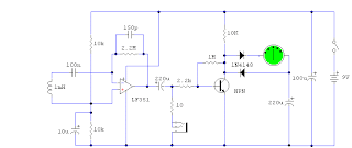
Here is a VLF receiver tuned to 300 kHz designed to detect the crackle of approaching lightning. A bright lamp flashes in synchrony with the lightning bolts indicating the proximity and intensity of the storm.

Follow The Instruction :

1) Figure 1 shows the simple receiver which consists of a tuned amplifier driving a modified flasher circuit. The flasher is biased to not flash until a burst of RF energy, amplified by the 2N3904, is applied to the base of the 2N4403. The receiver standby current is about 350 micro-amps which is nothing at all to a couple of D cells, hardly denting the shelf life. Of course, the stormier it gets, the shorter the battery life.


2) For best effect, mount the lamp in an old-fashioned holder with an extra-large colored glass lense. Or construct your own fixture with a plate of textured colored glass behind a panel painted with black-crackle paint. Watch a few old science fiction movies for other ideas.

3) A totally different approach is to mount the circuit in an empty glass jar with the antenna and bulb protruding through the top. (A malted-milk jar has a nice, red plastic lid which is easy to work and looks good.) Use a pin jack for the antenna. The gadget looks quite home-made but fascinating.

4) Boat owners may wish to replace the lamp with a 3-volt beeper to provide an early warning of approaching bad weather. Choose one of those unbreakable clear plastic jars like the large jars of coffee creamer. A little silicone rubber will seal the antenna hole in the lid of the jar. Use a longer antenna for increased sensitivity since there are few electrical noise sources on the lake.

5) Tune-up is simple: adjust the potentiometer until the regular flashing just stops. (Use a multi-turn trimmer.) When properly adjusted, the lamp will occasionally flash when large motors or appliances switch on and off and an approaching storm will give quite a show. Obviously, tune-up is a bit more difficult during stormy weather. Adjust the pot with no antenna if lightning is nearby. Tune an AM radio to the bottom of the dial to monitor the pulses that the lightning detector is receiving.
Conclusion:

This lightning detector is not so sensitive that it will flash with every crackle heard on the radio but will only flash when storms are nearby. Increased sensitivity may be achieved by increasing the antenna length. The experienced experimenter may wish to add another gain stage after the first by duplicating the 2N3904 circuitry including capacitor coupling with the addition of a 47 ohm emitter resistor to reduce the gain somewhat. This additional gain can cause stability problems if the layout is poor so novices are advised to use a longer antenna or adjust the sensitivity potentiometer more delicately instead! (When operating properly, the additional gain makes the pot adjustment much less critical.)

Sourch

Make a Electromagnetic Field Detector


Instruction:

This circuit is a real gem! Easy to make and more sensitive than many commercial devices available. It's based around an LF351 low-noise operational amplifier and a 1mF choke acting as the sensor. Unlike most other simple EMF detectors, this one has a meter output for accurate reading, but alternatively, you can also roughly estimate the frequency of the field by plugging in headphones. It can detect any field from 50Hz to 100kHz, making it highly versatile and a worthwhile addition to any hobbyist's workbench.


Use For :

Find out how far electromagnetic fields extend in your room, house, office...

Are you a ghost hunter? Then this is the circuit that you've been waiting for! Since it has been observed that appearance of a ghost tends to disturb the EMF, you can now detect any such changes with this little detector.

Digital Step-Km Counter

This circuit measures the distance covered during a walk. Hardware is located in a small box slipped in pants' pocket and the display is conceived in the following manner: the leftmost display D2 (the most significant digit) shows 0 to 9 Km. and its dot is always on to separate Km. from hm. The rightmost display D1 (the least significant digit) shows hundreds meters and its dot illuminates after every 50 meters of walking. A beeper (excludable), signals each count unit, occurring every two steps.

A normal step was calculated to span around 78 centimeters, thus the LED signaling 50 meters illuminates after 64 steps (or 32 operations of the mercury switch), the display indicates 100 meters after 128 steps and so on. For low battery consumption the display illuminates only on request, pushing on P2. Accidental reset of the counters is avoided because to reset the circuit both pushbuttons must be operated together.
Obviously, this is not a precision meter, but its approximation degree was found good for this kind of device. In any case, the most critical thing to do is the correct placement of the mercury switch inside of the box and the setting of its sloping degree.


Circuit operation:

IC1A & IC1B form a monostable multivibrator providing some degree of freedom from excessive bouncing of the mercury switch. Therefore a clean square pulse enters IC2 that divides by 64. Q2 drives the LED dot-segment of D1 every 32 pulses counted by IC2. Either IC3 & IC4 divide by 10 and drive the displays. P1 resets the counters and P2 enables the displays. IC1C generates an audio frequency square wave that is enabled for a short time at each monostable count. Q1 drives the piezo sounder and SW2 allows to disable the beep.
Notes:

* Experiment with placement and sloping degree of mercury switch inside the box: this is very critical.
* Try to obtain a pulse every two walking steps. Listening to the beeper is extremely useful during setup.
* Trim R6 value to change beeper sound power.
* Push P1 and P2 to reset.
* This circuit is primarily intended for walking purposes. For jogging, further great care must be used with mercury switch placement to avoid undesired counts.
* When the display is disabled current consumption is negligible, therefore SW3 can be omitted.

Sourch

Mobile or Telephone Phone Broadcaster

Hack mobile or telephone call by using phone broadcaster.

Here is a simple yet very useful circuit which can be used to eavesdrop on a telephone conversation. The circuit can also be used as a wireless telephone amplifier.

One important feature of this circuit is that the circuit derives its power directly from the active telephone lines, and thus avoids use of any external battery or other power supplies. This not only saves a lot of space but also money. It consumes very low current from telephone lines without disturbing its performance.


The circuit is very tiny and can be built using a single-IC type veroboard that can be easily fitted inside a telephone connection box of 3.75 cm x 5 cm. The circuit consists of two sections, namely, automatic switching section and FM transmitter section. Automatic switching section comprises resistors R1 to R3, preset VR1, transistors T1 and T2, zener D2, and diode D1. Resistor R1, along with preset VR1, works as a voltage divider.


When voltage across the telephone lines is 48V DC, the voltage available at wiper of preset VR1 ranges from 0 to 32V (adjustable). The switching voltage of the circuit depends on zener breakdown voltage (here 24V) and switching voltage of the transistor T1 (0.7V). Thus, if we adjust preset VR1 to get over 24.7 volts, it will cause the zener to breakdown and transistor T1 to conduct. As a result collector of transistor T1 will get pulled towards negative supply, to cut off transistor T2. At this stage, if you lift the handset of the telephone, the line voltage drops to about 11V and transistor T1 is cut off. As a result, transistor T2 gets forward biased through resistor R2, to provide a DC path for transistor T3 used in the following FM transmitter section.


The low-power FM transmitter section comprises oscillator transistor T3, coil L1, and a few other components. Transistor T3 works as a common-emitter RF oscillator, with transistor T2 serving as an electronic ‘on’/‘off’ switch. The audio signal available across the telephone lines automatically modulates oscillator frequency via transistor T2 along with its series biasing resistor R3. The modulated RF signal is fed to the antenna. The telephone conversation can be heard on an FM receiver remotely when it is tuned to FM transmitter frequency.


Lab Note: During testing of the circuit it was observed that the telephone used was giving an engaged tone
when dialed by any subscriber. Addition of resistor R5 and capacitor C6 was found necessary for rectification of the fault.

Sourch

Automatic Heat Detector Circuit .

This is a simple heat detector circuit based on NPN,PNP metallic transistor , IC UM3561 . This is easy to build and also a low-cost circuit.


We have added a table to enable readers to obtain all possible sound effects by returning pins 1 and 2 as suggested in the table.

By: SUKANT KUMAR BEHARA

Make a Clap Switch

There is a clap switch free from false triggering. To turn on or off any appliance, you just make clap twice. The circuit changes its output state only when you make clap twice within the set time period. Here, you’ve to clap within 3 seconds.

The amplified signal provides negative pulse to pin 2 of IC1 and IC2, triggering both the ICs. IC1, commonly used as a timer, is wired here as a monostable multivibrator. Trigging of IC1 causes pin 3 to go high and it remains high for a certain time period depending on the selected values of R7 and C3. This ‘on’ time (T) of IC1 can be calculated using the following relationship:

T=1.1R7.C3
seconds
where R7 is in ohms and C3 in microfar-
ads.


On first clap, output pin 3 of IC1 goes high and remains in this standby position for the preset time. Also, LED1 glows for this period. The output of IC1 provides supply voltage to IC2 at its pins 8 and 4.


Now IC2 is ready to receive the triggering signal. Resistor R10 and capacitor C7 connected to pin 4 of IC2 prevent false triggering when IC1 provides the supply voltage to IC2 at first clap.

On second clap, a negative pulse triggers IC2 and its output pin 3 goes high for a time period depending on R9 and C5. This provides a positive pulse at clock pin 14 of decade counter IC 4017 (IC3). Decade counter IC3 is wired here as a bistable.

Each pulse applied at clock pin 14 changes the output state at pin 2 (Q1) of IC3 because Q2 is connected to reset pin 15. The high output at pin 2 drives transistor T2 and also energises relay RL1. LED2 indicates activation of relay RL1 and on/off status of the appliance. A free-wheeling diode (D1) prevents damage of T2 when relay de-energises.

Circuit designed by: Mohammad Usamn Qureshi .

Sourch

A Transistor tester circuit

This is basically a high gain amplifier with feedback that causes the LED to flash at a rate determined by the 10u and 330k resistor. Remove one of the transistors and insert the unknown transistor. When it is NPN with the pins as shown in the photo, the LED will flash. To turn the unit off, remove one of the transistors.


Sourch

Black Light Project

This is a simple ultra-violate light circuit diagram that can be powered by a 6 volt battery or power supply that is capable of supplying 1 or more amps.


Parts Total Qty. Description
C1 1 0.0047uf Mono Capacitor
C2 1 0.1uf Disc Capacitor
D1, D2 2 1N4007 Diode
FTB 1 Filtered Blacklight Tube
IC1 1 555 Timer IC
P1 1 10k Trim Pot
Q1 1 TIP30 PNP Power Transistor
R1 1 470 Ohm Resistor
R2 1 270 Ohm Resistor
T1 1 Medium Yellow Inverter Transformer
MISC 1 IC Socket, Heat Sink For Q1, Screw, Nut, Wire and PC Board

Adjustable or Controllable Strobe Light

This is uses a much more powerful "Horse Shoe" Xenon tube. Which produces more light flash. You can control the flash rate up to about 20Hz. Do not look directly at the flash tube when this is running!


Parts:

R1 250 Ohm 10 Watt Resistor
R2 500K Pot
R3 680K 1/4 Watt Resistor
D1,D2 1N4004 Silicon Diode
C1, C2 22 uF 350V Capacitor
C3 0.47uF 400 Volt Mylar Capacitor
T1 4KV Trigger Transformer (see "Notes")
L1 Flash Tube (see "Notes")
L2 Neon Bulb
Q1 106 SCR
F1 115V 1A Fuse
Misc Case, Wire, Line Cord, Knob For R2


Note:

T1 and L1 are available from The Electronics Goldmine. This ciruits is NOT isolated from ground. Use caution when operating without a case. A case is required for normal operation. Do not touch any part of the circuit with the case open or not installed. Most any diodes rated at greater then 250 volts at 1 amp can be used instead of the 1N4004's. Do not operate this circuit at high flash rates for more than about 30 seconds or else C1 and C2 will overheat and explode. There is no on/off switch in the schematic, but you can of course add one.
Sourch

CHRISTMAS STAR By MAINS-OPERATED

There is a low cost circuit diagram of Christmas star that can be easily maked even by a novice. The main advantage of this circuit is that it does not equire any step-down transformer or ICs.


Parts List:
R1 ------------------ 100 ohm
R2 ------------------ 100 ohm
R3 ------------------ 10 ohm
R4 ------------------ 100K
R5 ------------------ 100K
R6 ------------------ 10K
R7 ------------------ 10K
C1 ------------------ 0.1µ
C2 ------------------ 220µ
C3 ------------------ 0.1µ
C4 ------------------ 47µ
C5 ------------------ 47µ
D1 ------------------ 1N4007
D2 ------------------ 1N4007
D3 ------------------ 1N4007
ZD1 ---------------- 5.6V
LED1 -------------- Any
T1 ------------------- BC548
T2 ------------------- BC548
T3 ------------------- BC548
MT1,MT2 --------- BT136

Circuit Design By: PRINCE PHILLIPS


Sourch

Telephone call Voice Changer Circuit

If your ask is that ...
How to make a telephone call voice changer circuit ?
 2) How to make a phone call voice changer circuit?
 3)How to convert male voice to female voice ?
This is a simple telephone call voice changer circuit . You can change male voice to famale voice by using this circuit diagram.


Parts :

P1______________10K Log. Potentiometer

R1,R10__________10K 1/4W Resistors
R2_______________1K 1/4W Resistor
R3______________50K 1/2W Trimmer Cermet or Carbon
R4,R6,R7,R14___100K 1/4W Resistors
R5______________47K 1/4W Resistor
R8______________68K 1/4W Resistor
R9_______________2K2 1/2W Trimmer Cermet or Carbon
R11_____________33K 1/4W Resistor
R12_____________18K 1/4W Resistor
R13_____________15K 1/4W Resistor
IC1___________LM358 Low Power Dual Op-amp
IC2_________TDA7052 Audio power amplifier IC

MIC1__________Miniature electret microphone

SPKR______________8 Ohm Small Loudspeaker

SW1____________DPDT Toggle or Slide Switch
SW2,SW3________SPST Toggle or Slide Switches


C1,C2,C3,C8,C9_100nF 63V Polyester Capacitors
C4______________10µF 25V Electrolytic Capacitor
C5_____________220nF 63V Polyester Capacitor (Optional, see Notes)
C6_______________4n7 63V Polyester Capacitor
C7______________10nF 63V Polyester Capacitor
C10____________220µF 25V Electrolytic Capacitor


J1____________6.3mm or 3mm Mono Jack socket

B1_______________9V PP3 Battery (See Notes)

Clip for PP3 Battery

This design fulfills these requirements by means of a variable gain microphone preamplifier built around IC1A, a variable steep Wien-bridge pass-band filter centered at about 1KHz provided by IC1B and an audio amplifier chip (IC2) driving the loudspeaker.

Notes:

1) The pass-band filter can be bypassed by means of SW1A and B: in this case, a non-manipulated microphone signal will be directly available at the line or loudspeaker outputs after some amplification through IC1A.

2) R3 sets the gain of the microphone preamp. Besides setting the microphone gain, this control can be of some utility in adding some amount of distortion to the signal, thus allowing a more realistic imitation of a telephone call voice.

3) R9 is the steep control of the pass-band filter. It should be used with care, in order to avoid excessive ringing when filter steepness is approaching maximum value.

4) P1 is the volume control and SW2 will switch off amplifier and loudspeaker if desired.

5) C5 is optional: it will produce a further band reduction. Some people think the resulting effect is more realistic if this capacitor is added.

6) If the use of an external, moving-coil microphone is required, R1 must be omitted, thus fitting a suitable input jack.

7) This circuit was intended to be powered by a 9V PP3 battery, but any dc power supply in the 6 - 12V range can be used successfully.

Sourch

Telephone Sharer circuit 9 channel

Introduction:

This circuit is able to handle nine independent telephones (using a single telephone line pair) located at nine different locations, say, up to a distance of 100m from each other, for receiving and making outgoing calls, while maintaining conversation secrecy. This circuit is useful when a single telephone line is to be shared by more members residing in different rooms/apartments.
Description:

Normally, if one connects nine phones in parallel, ring signals are heard in all the nine telephones (it is also possible that the phones will not work due to higher load), and out of nine persons eight will find that the call is not for them. Further, one can over- hear others’ conversation, which is not desirable. To overcome these problems, the circuit given here proves beneficial, as the ring is heard only in the desired extension, say, extension number ‘1’.

Sourch

For making use of this facility, the calling subscriber is required to initially dial the normal phone number of the called subscriber. When the call is established, no ring-back tone is heard by the calling party. The calling subscriber has then to press the asterik (*) button on the telephone to activate the tone mode (if the phone normally works in dial mode) and dial extension number, say, ‘1’, within 10 seconds. (In case the calling subscriber fails to dial the required extension number within 10 seconds, the line will be disconnected automatically.) Also, if the dialed extension phone is not lifted within 10 seconds, the ring-back tone will cease.


Operation:

The ring signal on the main phone line is detected by opto-coupler MCT- 2E (IC1), which in turn activates the 10-second ‘on timer’, formed by IC2 (555), and energises relay RL10 (6V, 100- ohm, 2 C/O). One of the ‘N/O’ contacts of the relay has been used to connect +6V rail to the processing circuitry and the other has been used to provide 220-ohm loop resistance to de-energise the ringer relay in telephone exchange, to cut off the ring.


When the caller dials the extension number (say, ‘1’) in tone mode, tone receiver CM8870 (IC3) outputs code ‘0001’, which is fed to the 4- bit BCD-to-10 line decimal de- coder IC4 (CD4028). The output of IC4 at its output pin 14 (Q1) goes high and switches on the SCR (TH-1) and associated relay RL1. Relay RL1, in turn, connects, via its N/O contacts, the 50Hz extension ring signal, derived from the 230V AC mains, to the line of telephone ‘1’. This ring signal is available to telephone ‘1’ only, because half of the signal is blocked by diode D1 and DIAC1 (which do not conduct below 35 volts).

As soon as phone ‘1’ is lifted, the ring current in- creases and voltage drop across R28 (220-ohm, 1/2W resistor) increases and operates opto-coupler IC5 (MCT-2E). This in turn resets timer IC2 causing:


(a) interruption of the power supply for processing circuitry as well as the ring.

A small FM transmitter

This FM transmitter has an operating frequency of about 80 to 115MHz. Under reasonable circumstances you will be able to receive its signal at a distance of about 200 meters. Although it is low-power, it might be illegal in your part of the planet.


Sourch

Make a TV Transmitter

One of the most useful gadgets a video enthusiast can have is a low-power TV Transmitter. Such a device can transmit a signal from a VCR to any TV in a home or backyard. Imagine the convenience of being able to sit by the pool watching your favorite movie on a portable with a tape or laserdisc playing indoors. You could even retransmit cable TV for your own private viewing. Videotapes can be dubbed from one VCR to another without a cable connecting the two machines together.

When connected to a video camera, a TV transmitter can be used in surveillance for monitoring a particular location. The main problem a video enthusiast has in obtaining a TV transmitter is that a commercial units are expensive. However, we have some good news! You can build the TV Transmitter described here for less than $30 in one evening! The easiest way to do that is to order the kit that‚s available from the source given in the Parts List (a custom case for the kit is also available). Nevertheless, we present enough information here to build the TV Transmitter from scratch.
The TV Transmitter combines line- level audio and video signals, and transmits the resulting signal up to 300 feet. The circuit can be powered from a 9- volt battery. It is suggested that a 12-volt DC supply during be used during the alignment procedure. This would insure maximum transmission range and best possible picture. Aligning the TV Transmitter requires no special equipment whatsoever, and it is a very simple procedure. The Transmitter's output can be tuned to be received on any TV channel from 2 to 6. The range of channels is wide enough so that the unit will not interfere with other TV viewers who are nearby. To comply with FCC rules, it is mandatory the nearby TV viewers are not disturbed by the transmission. If your activities interfere with the reception from a licensed station, regardless of the reason, you must shut down your unit.


Circuit Description:


Figure 1 is the schematic diagram of the TV Transmitter circuit. Video signals input at jack J1 are first terminated by resistor R6 and coupled through capacitor C1 to clamping-diode D1. The clamping forces the sync pulses to a fixed DC level to reduce blooming effects. Potentiometer R3 is used to set the gain of the video signal; its effect is similar to that of the contrast control on a TV set. Bias-control R7 can be used to adjust the black level of the picture so that some level of signal is transmitted, even for a totally dark picture. That way, a TV receiver can maintain proper sync. As we'll get to later, potentiometers R3 and R7 are cross adjusted for the best all-around performance.

RF-transformer T1 and its internal capacitor form the tank circuit of a Hartley oscillator that's tuned to 4.5 megahertz. Audio signals input at J2 are coupled to the base of Q3 via C2 and R4: the audio signal modulates the base signal of Q3 to form an audio subcarrier that‚s 4.5-megahertz higher than the video-carrier frequency. The FM modulated subcarrier is applied to the modulator section through C5 and R9. Resistor R9 adjusts the level of the subcarrier with respect to the video signal. Transistors Q1 and Q2 amplitude modulate the video and audio signals onto an RF-carrier signal. The operating frequency is set by coil L4, which is 3.5 turns of 24- gauge enameled wire on a form containing a standard ferrite slug.

That coil is part of a Colpitts tank circuit also containing C7 and C9. The tank circuit forms Q4's feedback network, so Q4 oscillates at the set frequency The RF output from the oscillator section is amplified by Q5 and Q6, whose supply voltage comes from the modulator section. Antenna matching and low-pass filtering is performed by C12, C13, and L1. Resistor R12 is optional; it is added to help match the output signal to any kind of antenna. (More on that in a moment.)


 PARTS LIST FOR THE
TV TRANSMITTER

SEMICONDUCTORS

D1—1N914 silicon diode
Q1-Q—2N3904 NPN transistor
RESISTORS
(All fixed resistors are 1/4-watt, 5% units .)
R1, R2, R11—1000-ohm
R3, R7—1000-ohm trimmer potentiometer, PC-
mount
R4, R9, R10—10,000-ohm
R5—47,000-ohm
R6—75-ohm
R8—4700-ohm
R12—75-ohm (optional, see text)

CAPACITORS

C1, C8—100-µF, 16-WVDC, electrolytic
C2—2.2--µF, 50-WVDC, electrolytic
C3-C6, C11, C14, C15—001-µF, ceramic-disc
C7, C9—2.2-pF, ceramic-disc
C10—100-pF, ceramic-disc
C12, C13—68-pF, ceramic-disc

ADDITIONAL PARTS AND MATERIALS

ANT1—Antenna, telescopic-whip
B1—9-volt battery
J1-J3—RCA jack, PC-mount
L1—0.15-µH miniature inductor
L2, L3—2.2-µH miniature inductor
L4—0.14- to 0.24-mH adjustable, slug-tuned coil
(see text)
S1—SPST, push-button switch, normally open
T1—4.5-MHz 1F-can-style RF  transformer (see
text)
Printed-circuit materials or pre-fab PC board,
battery holder and connector, pair of RCA
patch cords, solder, hardware, etc.
Note: The following items are available from
     Ramsey Electronics, Inc.
     793 Canning Parkway
     Victor, NY  14564
     Tel. 716-924-4560
TV-6 TV Transmitter Kit (includes PC board and all
components except R12)—$27.95; kit of all
components (except R12)—$17.95; PC board
only—$10.00; CTV matching-case set—$14.95.
NY State residents please add appropriate sales
tax.

Sourch

TV-Transmitter

A VHF band TV transmitter using negative sound modulation and PAL video modulation. This is suitable for countries using TV systems B and G.


Notes: The frequency of the transmitter lies within VHF and VLF range on the TV channel, however this circuit has not been tested at UHF frequencies. The modulated sound signal contains 5.5 -6MHz by tuning C5. Sound modulation is FM and is compatible with UK System I sound. The transmitter however is working at VHF frequencies between 54 and 216MHz and therefore compatible only with countries using Pal System B and Pal System G.

For more information on TV systems visit the links below:

Television Frequency Table
Televison system frequency and channel standards.

Sourch

Make a FM Booster

There is a low-cost circuit of an FM booster which can be used to listen programmes from high distant FM stations clearly.
The circuit comprises a common-emitter tuned RF preamplifier wired around VHF or UHF transistor 2SC2570. (Only C2570 is annotated on the transistor body.)


Parts List:
R1 ---------------------------------- 27K
R2 ---------------------------------- 270K
R3 ---------------------------------- 1K
C1 ---------------------------------- 5.6p
C2 ---------------------------------- 5.6p
C3 ---------------------------------- 1n
C4 ---------------------------------- 10p
C5 ---------------------------------- 10p
C6 ---------------------------------- 0.1micro
VC1 -------------------------------- 22p
VC2 -------------------------------- 22p
T1 ----------------------------------- C2570
L1 ----------------------------------- 20SWG ( 4 Turns ; 5mm diameter)
L2 ----------------------------------- 20SWG ( 3 turns ; 5mm diameter)

Sourch